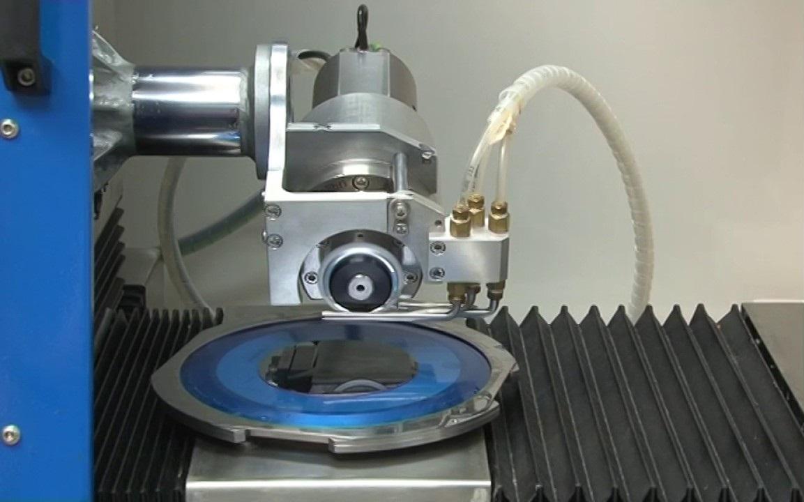
Wafer Dicing serves several essential purposes in semiconductor manufacturing:
-
Individual Component Creation: Semiconductor wafers typically contain numerous identical semiconductor devices or integrated circuits (ICs) that are created simultaneously during the wafer fabrication process. Dicing allows these devices to be separated into individual chips, each of which can function as an independent electronic component.
-
Packaging: Separated chips are easier to handle and package. Packaging provides protection from environmental factors, electrical connections for interfacing with other components, and mechanical support for handling and mounting in electronic devices.
-
Testing and Quality Control: Diced chips can be individually tested and inspected to ensure they meet quality and performance standards. This level of granularity in testing allows manufacturers to identify and reject defective chips, ensuring only functional components are used in electronic devices.
-
Customization: Dicing allows for customization of semiconductor products. Different chips on a wafer may have varying functionalities or specifications, and by dicing, manufacturers can select and use the chips that meet the specific requirements of their electronic devices.
-
Efficiency and Yield: Dicing can improve manufacturing efficiency and yield. If a defect is found in one part of the wafer, only the affected area needs to be discarded, while the rest of the wafer remains usable. This reduces waste and maximizes the yield of functional chips from each wafer.
-
Size and Form Factor: Diced chips can be made in various sizes and form factors to suit different applications. Some electronic devices require small, compact chips, while others may use larger chips. Dicing allows for flexibility in producing chips of different sizes and shapes.
-
Ease of Handling: Diced chips are easier to handle during assembly and integration into electronic devices. They are typically more robust and less prone to damage compared to a fragile wafer, making the manufacturing process more manageable.
-
Repair and Redundancy: In certain cases, if a defect or failure is detected in a packaged semiconductor device, it may be possible to replace it with a spare or redundant chip, which can be created by dicing the wafer. This can enhance the reliability and serviceability of electronic systems.
In summary, dicing a semiconductor wafer is a critical step in the manufacturing process that transforms a large, complex wafer into individual, functional semiconductor chips. This enables efficient testing, packaging, customization, and integration of these chips into a wide range of electronic devices, ultimately contributing to the production of high-quality and reliable electronics.